Author Profile
Alex Turner is a senior PCB design engineer with 12+ years in power electronics. He specializes in high-current connector layout, has designed PCBs for drones, EV modules and portable power systems, and holds certifications in IPC-A-600 and IPC-2221. He has optimized over 200 connector footprints to improve thermal and mechanical stability.
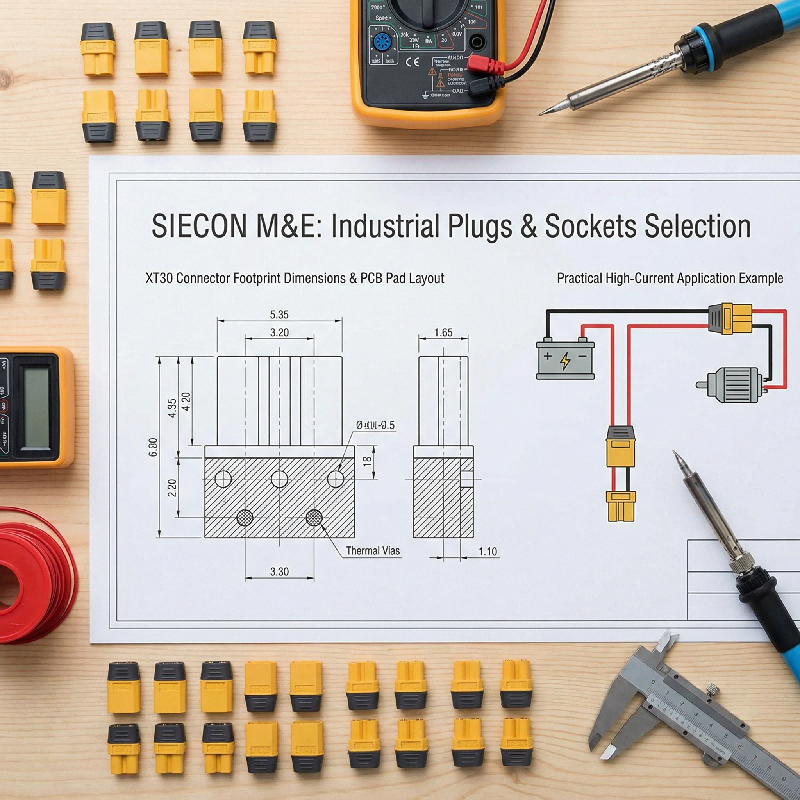
What Is the Power XT30 Connector Footprint
The power XT30 connector footprint defines pad size and hole position on PCBs. It supports stable high-current transmission in compact electronic devices. Standard dimensions ensure mechanical fit and soldering reliability in mass production.
Key Mechanical Dimensions of XT30 Footprint
Accurate pin spacing and pad diameter are critical for XT30 footprint performance. Deviations in hole size can cause loose fitting or cold solder joints. Industry-standard dimensions prevent assembly failure in batch production.
Thermal Design for Power XT30 Connector Footprint
Thermal copper expansion improves heat dissipation in high-current XT30 applications. Proper thermal vias reduce temperature rise during continuous power loading. This design avoids overheating in drone and battery circuits.
PCB Layout Best Practices for XT30 Footprint
Keep XT30 footprint away from noise-sensitive analog and signal components. Shorten power traces to reduce resistance and voltage drop in the circuit. Maintain safe clearance to meet high-voltage insulation standards.
Real-World Case: Drone Power Module XT30 Layout
A drone manufacturer faced overheating with an undersized XT30 footprint. Enlarging thermal pads and adding vias reduced operating temperature by 18°C. The revised layout passed 24-hour continuous load testing successfully.
Second Engineering Case: Portable Power Station
A portable power station suffered loose XT30 connections under vibration. Optimized footprint pad shape and solder mask improved mechanical retention. The product then passed shock and vibration reliability tests.
SMT and Through-Hole Considerations for XT30 Footprint
XT30 footprints typically use through-hole pads for stronger mechanical bonding. Solder fillet size directly affects long-term vibration and pull resistance. Controlled soldering profiles prevent pad lifting or solder bridging.
Common Mistakes in XT30 Connector Footprint Design
Many designers use generic footprints that mismatch actual XT30 part dimensions. Insufficient thermal relief causes soldering difficulties and weak joints. Ignoring trace width leads to excessive resistance and power loss.
Verification and Validation of XT30 Footprint
Use 3D assembly simulation to check mechanical fit of the XT30 connector. Conduct thermal imaging to validate heat distribution under full load. Perform pull tests to confirm long-term connection reliability.
Final Design Recommendations for XT30 Footprint
Always reference official manufacturer datasheets for XT30 footprint values. Combine thermal design and mechanical stability for harsh-environment use. Test prototypes before mass production to avoid redesign costs.