The 5V SMPS remains the workhorse of modern electronics, powering everything from microcontrollers to sensors. Designing a reliable requires more than just schematic capture; it demands a deep understanding of topologies and parasitic elements. In my fifteen years as a power supply design engineer, I have witnessed countless project delays caused by overlooked fundamentals. This article aims to bridge the gap between theory and practical, manufacturable designs. We will explore the intricacies of the flyback converter, which is the most popular choice for low-power applications. Furthermore, we will dissect real-world issues like output ripple and thermal management. My goal is to provide you with actionable insights that stem from direct laboratory experience. Let us begin by understanding why the 5V rail is so critical in system design.
Why the 5V SMPS is the Universal Standard for Digital Logic
The 5V logic level has been a cornerstone of embedded systems since the inception of TTL logic families. Even with the proliferation of 3.3V and lower voltage devices, the 5V SMPS remains essential for powering sensors, motors, and communication interfaces. Many industrial control systems still operate primarily on a 5V SMPS to ensure noise immunity and compatibility with legacy hardware. For instance, the Intel Galileo board specifically requires a regulated 5V supply capable of delivering up to 3A. This demand for clean, stable power highlights the importance of proper regulation. Without a well-designed, microcontrollers may experience erratic behavior or complete failure. Therefore, mastering this specific voltage rail is a fundamental skill for any power electronics engineer.
Topology Selection: Why the Flyback Converter Dominates Low-Power 5V SMPS
When designing a 5V SMPS for under 50 watts, the flyback converter topology is often the default choice. Its popularity stems from its simplicity and low component count, which directly reduces bill of materials costs. A typical flyback utilizes a single switching transistor and a coupled inductor, simplifying the design significantly. Research has demonstrated that a utilizing a flyback converter can be effectively constructed using readily available components like the 555 timer. This topology inherently provides isolation between the input AC mains and the sensitive 5V output. Isolation is critical for user safety and for preventing ground loops in sensitive audio or measurement equipment. However, the flyback converter does have a drawback: it tends to produce higher output ripple compared to forward converters. Despite this, its cost-effectiveness makes it the winner for applications like phone chargers and auxiliary power supplies.
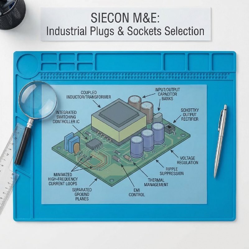
The Importance of the Transformer in Flyback 5V SMPS Design
The transformer, or coupled inductor, is the heart of any flyback. Unlike a normal transformer, it stores energy in its air gap during the switch on-time and releases it to the output during the off-time. Designing this magnetic component requires careful calculation of primary inductance and turns ratio. A poor transformer design will lead to saturation and catastrophic failure of the MOSFET. In a 5V SMPS, the secondary winding must be precisely wound to achieve the correct voltage ratio. I always recommend using Litz wire for the secondary winding to minimize skin effect losses. Furthermore, the leakage inductance must be minimized through proper winding techniques to reduce voltage spikes. These design decisions directly impact the efficiency and reliability of your 5V SMPS.
Real-World Design Example: Achieving 5V at 2A with Peak Power Handling
Let us examine a practical implementation of a 5V SMPS using a dedicated controller IC. The STEVAL-ISA125V1 reference design from STMicroelectronics provides an excellent example of a robust 5V, 2A supply. This particular 5V SMPS utilizes the VIPer28LN converter, which integrates an 800 V avalanche-rugged MOSFET. A key feature of this design is its ability to handle peak loads of up to 3A for short durations. This is crucial for applications like printers or audio systems where the load demands sudden surges of power. The design achieves this through the Enhanced Peak Power (EPT) function, which prevents thermal overload. It operates at a 60 kHz switching frequency with jittering to reduce EMI signatures. By studying such reference designs, engineers can understand how to balance continuous power ratings with peak demands.
Analyzing the Specifications of Reference Design
When evaluating a 5V SMPS reference design, you must look beyond just the output voltage. The STEVAL-ISA125V1 specifies an input range from 90 VAC to 265 VAC, making it suitable for global use. The output regulation precision is rated at ±5%, which is adequate for most digital loads. High-frequency ripple is specified at 50 mV, a figure that requires careful output capacitor selection to achieve. The maximum ambient operating temperature of 60°C dictates the thermal management strategy required. These specifications serve as a benchmark for your own 5V SMPS designs. Always cross-validate your calculated values against such proven examples.
Taming the Noise: Techniques for Ripple Reduction
One of the biggest challenges in 5V SMPS design is minimizing output voltage ripple. Digital loads require clean power, and excessive ripple can corrupt data conversion or logic states. A common technique to combat this is the use of a cascaded low-dropout regulator. By placing an LDO after the 5V SMPS output, you can achieve significant ripple rejection. Studies show that cascading an LDO can improve Power Supply Rejection Ratio by over 46 dB at certain frequencies. The LDO effectively filters out the switching artifacts generated by the SMPS. However, this comes at the cost of slight efficiency loss due to the LDO’s dropout voltage. For ultra-sensitive analog circuits, this trade-off is absolutely necessary. Therefore, knowing when to add post-regulation is a mark of an experienced designer.
PCB Layout Strategies for a Low-Noise 5V SMPS
The physical layout of your 5V SMPS is just as important as the schematic. High-frequency current loops, particularly those involving the transformer and MOSFET, must be kept extremely small. A poor layout will radiate EMI and introduce noise into the ground plane. For the 5V output side, the trace connecting the output capacitor to the load must be wide and short. I always use a dedicated ground plane for the control circuitry to separate it from power ground. The feedback trace, which senses the 5V output, must be routed away from magnetic components. Connecting this trace at the output capacitor rather than the inductor ensures accurate voltage sensing. Neglecting these layout rules is the primary reason why a 5V SMPS works in simulation but fails in the lab.
Thermal Management: Keeping Your 5V SMPS Cool Under Pressure
Thermal stress is the enemy of reliability in any 5V SMPS. The efficiency of the converter dictates how much heat must be dissipated. For example, if a 5V SMPS is outputting 5W at 93% efficiency, the power loss is approximately 0.35W, which turns into heat. This heat must be conducted away from the IC and MOSFET to prevent thermal shutdown. In open-frame designs like the RECOM RACM60-K series, convection cooling is often sufficient up to +55°C. For higher ambient temperatures, forced air cooling or derating is required. The VIPer devices from ST include thermal shutdown with hysteresis to protect the 5V SMPS during fault conditions. As a designer, you must calculate the junction temperature of your switching IC under worst-case conditions. Proper heatsinking and PCB copper pours are essential for extracting heat from the components.
Component Selection: Choosing the Right Diode and Capacitors for 5V SMPS
The output rectifier diode in a 5V SMPS experiences significant stress. For low-voltage outputs like 5V, Schottky diodes are preferred due to their low forward voltage drop. A lower drop directly translates to higher efficiency and less heat generation. On the input side, the bulk capacitor must handle the ripple current without overheating. The capacitor’s lifetime is directly related to its core temperature; for every 10°C rise, the lifespan often halves. In the STVial 5V SMPS designs, the bill of materials includes capacitors with specific ESR ratings. Using generic capacitors with high ESR will result in increased output ripple. Always select components rated for the switching frequency of your 5V SMPS. This attention to detail separates a prototype from a production-ready power supply.
Efficiency Optimization Across the Load Range
Modern energy regulations demand that a 5V SMPS be efficient not only at full load but also at light loads. The Eco-design directives require standby power to be less than 0.5W in many applications. To achieve this, controllers now employ features like burst mode operation at light loads. This reduces switching losses by operating in short bursts followed by long sleep periods. The VIPer114B, for instance, is designed for low-power 5V SMPS applications with very low standby consumption. Efficiency at 10% load is becoming a key specification for appliance power supplies. Therefore, selecting a controller with advanced power-saving modes is crucial for compliance. A truly optimized 5V SMPS will maintain high efficiency across its entire operating range.
The Role of Synchronous Rectification in 5V SMPS
For 5V SMPS designs requiring very high current, such as 8A, synchronous rectification is indispensable. Replacing the Schottky diode with a low-RDS(on)RDS(on) MOSFET dramatically reduces conduction losses. The NXP full-bridge DC-DC reference design utilizes synchronous rectification on the secondary side to achieve high efficiency. This technique is more complex because it requires precise timing to drive the MOSFETs. However, the gain in efficiency, often several percentage points, is worth the complexity for high-current 5V SMPS modules. The reduction in heat also allows for higher power density in compact enclosures.
Testing and Validation: Simulating Your 5V SMPS Before Building It
Before soldering a single component, simulating your 5V SMPS can save weeks of debugging. Software tools like PSIM allow designers to model the behavior of the power stage and feedback loop. One academic project successfully used PSIM to simulate a triple-output SMPS before hardware implementation. Simulation helps you visualize the switch node waveforms and verify that the inductor does not saturate. It also allows you to check the control loop stability by plotting the Bode plot. Tools from manufacturers like MPS even provide pre-validated waveforms and efficiency graphs for their 5V SMPS designs. Always simulate your design under startup, steady-state, and short-circuit conditions. This proactive approach ensures that your physical 5V SMPS will perform as expected.
Conclusion: The Path to 5V SMPS Mastery
Designing a robust and efficient 5V SMPS is a blend of science and art. We have explored the importance of topology selection, with the flyback converter taking center stage for low-power applications. We dissected the thermal and noise challenges that every designer faces in the laboratory. By learning from detailed reference designs, such as those from ST and NXP, you can avoid common pitfalls. Remember that the PCB layout and component selection are just as critical as the theoretical calculations. As you embark on your next 5V SMPS project, apply these principles diligently. The demand for reliable 5V power will only grow with the expansion of IoT and embedded devices. Master this domain, and you will become an indispensable asset to any engineering team.